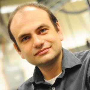
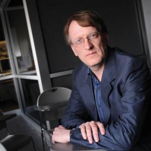
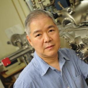
Harish Krisnaswamy’s Startup, MixComm, Acquired for $155M
Semiconductor company builds mm-wave chips that power infrastructure for 5G networks
More
Oct 20 2021 | By Holly Evarts
Semiconductors are the foundational technology of the digital and information age and continued investment in manufacturing, research and development, and workforce development–supported through strong partnerships and collaboration–is critical to the growth of the semiconductor technology ecosystem.
Columbia Engineering brings forward a convergent vision that considers all aspects of semiconductor technology, manufacturing, and talent development. Our people, our culture, and innovative educational and training programs are fundamental to our success in facilitating high-impact university-industry and public partnerships. Our expertise in building large-scale, multi-institute centers make it easier for our researchers and students to work across disciplines, departments, institutions, and industry to address big problems that no single lab or company could tackle.
With our best-in-class research, cutting-edge facilities, hands-on educational and training programs, and commitment to increased diversity and equity, we are training the next generation of talent to drive innovation in the semiconductor technology ecosystem.


Columbia brings leading and unparalleled strengths in the following key research areas:
Nanophotonics can provide high bandwidth, high speed, and ultra-small optoelectronic components. This technology has the potential to revolutionize telecommunications, computation, and sensing. Columbia Engineering is well-positioned as the leading institute for the investigation of the physics and applications of nanoscale photonic structures with the ability to bring photonic optics to the chip scale (silicon photonics), combining them with electronic systems for many future applications. Research strengths include multiple programs on optical interconnection networks for advanced computing systems, data centers, optical packet-switched routers, and nanophotonic networks-on-chip for chip multiprocessors. With the growing demand for photonics-based technologies in data centers and high-performance computing applications, our research aims to be on the cutting edge of research while creating feasible and deployable solutions to tackle real challenges faced in industry.
Columbia University has a leading research portfolio in advanced wireless, with research spanning integrated circuits, communication systems, and networking. Areas of research include all technologies within emerging wireless, such as wideband and cognitive radio, low-power internet-of-things, millimeter-wave/terahertz wireless, massive MIMO, and full-duplex wireless. Our multiple leading projects in this research are funded by diverse sources, including NSF, DARPA, and industry (SRC and others). In addition to the SRC JUMP 2.0 center, which has about a key focus on wireless, Columbia Engineering leads the NSF PAWR COSMOS testbed, a ~$25M NSF-funded program setting up an advanced city-scale wireless testbed for broader community use. Columbia Engineering’s recently-awarded NSF ERC on smart cities, led by Professor Andrew Smyth, also focuses on wireless for smart cities.
Design integrated circuits. Historically regarded as a global and academic leader in integrated-circuit design, Our research program spans all areas of IC design, including low-power and high-complexity digital circuits and systems, analog and mixed-signal circuits, RF/millimeter-wave/terahertz integrated circuits, cryogenic circuits for quantum applications, and bioelectronics. Columbia’s research program is funded by diverse sources, including NSF, DARPA, industry (SRC and others), and NIH. Our research facilities include four leading labs spanning each area featuring multi-million dollar institutional infrastructure investments. Application areas include wireless (5G and beyond), high-performance computing, and quantum and bio applications.
Columbia Engineering offers a highly recognized and comprehensive program to train next-generation engineers to design integrated circuits (chips). Columbia Engineering undergraduate students can follow a depth area in “Circuits and Electronics.” Masters students can elect to do a specialization in Integrated Circuits and Systems. We have seen a substantial increase in our enrollments in this area. The Department of Electrical Engineering’s EE6350 VLSI Design Lab, taught by Professor Peter Kinget, is a highly unique course that teaches students how to design an actual chip in the spring semester, gets fabricated in the summer semester (funded by Apple Inc.), and that the students test in the fall semester.
Columbia Engineering also brings significant strength in nanoscale structures and integrated devices. This research applies fundamental physical principles to develop revolutionary new electronic, photonic, and optical devices made from conventional and emerging materials, including graphene, 2D semiconductors, and organic semiconductors. Research includes nanofabrication, characterization, and electromagnetic design of quantum device structures and complex silicon photonic circuits that impact numerous fields, from Lidar and optogenetics to low-energy computation and flexible electronics. In addition to projects in CMOS integrated sensor solutions, Professor John Kymissis focuses on thin film electronics, particularly in the applications of organic semiconductors, thin film piezoelectric, and recrystallized silicon devices.
Open-source hardware has the potential to play a uniquely instrumental role in the age of heterogeneous computing. Columbia Engineering brings significant leadership in developing open-source software and hardware and releasing it in the public domain. Most recently, Professor Luca Carloni led essential contributions to the QEMU project. In particular, they developed and released ESP, among the first open-source research platforms for heterogeneous system-on-chip (SoC) design and programming. Besides fostering the much-needed development of new workforce generations in various areas of computer engineering, this area also holds the promise of democratizing hardware development, thus opening new opportunities for broadening the participation and engagement of members of underrepresented minorities. As an example of Columbia Engineering’s innovative educational contributions, the “System-on-Chip Platforms” course prepares students to contribute to the new economy of heterogeneous computing and open-source hardware. The course, offered every academic year since 2013, was one of the first nationwide to introduce commercial high-level synthesis tools for the design of application-specific hardware accelerators.
A key area highlighted in the planning documents for the NSTC, bioelectronics, includes the applications of integrated circuit technology to the life sciences. Bioelectronics requires "more-than-Moore" updates to traditional CMOS processes while relying almost entirely on legacy semiconductor nodes. Led by the research efforts of Professor Ken Shepard, our research creates a unique opportunity to exploit lower-end nodes for new markets –making this a key strategic opportunity for collaboration between universities and start-up companies. In particular, there is significant growth opportunity in molecular diagnostics and neurotech, both of which Columbia has a leading presence.
Columbia Engineering also brings significant research leadership in power electronics, battery management systems, and motor control for electric vehicle and grid applications. Professor Matthias Preindl’s lab group focuses on the design and control of power electronic systems, motor drive systems, and energy storage systems for transportation electrification and a sustainable power system. His group has introduced software-defined power converters and high-performance Lego-like power electronics modules. This research leverages wide-bandgap semiconductors (SiC MOSFTETs and GAN HEMTs) to reduce power losses and volume by a factor 5-10. Leveraging the resources of Columbia’s Electro Chemical Engineering Center (CEEC), Data Science Institute, Columbia’s Formula Racing (CUFR) team, and Climate School, the Priendl Lab has unique strengths in leveraging controls (software) to operate wide bandgap devices (hardware) in ways that benefit a system (EV for example) coupled with real-time model predictive control, estimation, and machine learning with microsecond execution times.
Columbia develops, manages, operates, and maintains a world-class set of user-shared lab facilities to support nanoscale science and engineering research activities, making these available to the entire Columbia community at a modest cost. These lab facilities currently include a Clean Room for micro- and nanofabrication, a Materials Characterization Facility, and an Electron Microscopy Facility. The research facilities are also open to external users from other academic institutes and industrial companies. Through the Columbia Nano Initiative (CNI), we collaborate with other universities, such as CUNY, to make additional capabilities available to the entire Columbia research community, industry partners, and beyond.
Converging Columbia’s unique strengths in photonics, wireless, and electronics, the recently awarded SRC JUMP 2.0 brings together a multi-PI, multi-university center (~$35M) to address the critical problem of the connectivity bottleneck, across diverse commercial and defense platforms, in scaling today’s information processing systems to handle the explosive growth in data-intensive applications. Led by Professor Keren Bergman, a pioneer in photonic interconnected computing with extensive experience leading large programs (currently DARPA PIPES and ARPA-E), CUbiC brings together a world-class team of PIs —with expertise that spans the full systems-to-devices ‘stack’ in communications and connectivity— to collaborate deeply to realize its ambitious vision of demonstrating a new communication paradigm. CUbiC will develop connectivity and communications technologies that scale to meet the needs of emerging distributed data-centric applications. In addition, leveraging the NSF COSMOS Platform for Advanced Wireless Research Center, CUbiC provides the first-in-class testbed for system-level validation that industry partners can utilize for next-generation technologies and applications demo and training opportunities. With shared purpose emphasized by carefully cultivated collaboration across key research strengths, the center aims to realize end-to-end connectivity at > 10 Tb/s with energy efficiencies of < 100 fJ/bit while extending reach by >10× and enhancing bandwidth densities by >100× over bandwidth-constrained channels.
Building upon and maintaining Columbia’s strong and successful experiences with highly multidisciplinary and collaborative research programs in Nanoscale Science and Engineering, Columbia University’s Columbia Nano Initiative (CNI) stimulates the development of new major research centers and programs and assures the creation and maintenance of the specialized facilities that support and enable these groundbreaking programs. CNI represents an interdisciplinary community within Columbia University dedicated to supporting and developing research efforts in Nanoscale Science and Engineering. Beyond providing the faculty-based intellectual basis and support for the development of new research concepts, directions, and programs in nanoscience and nanotechnology, CNI provides an administrative and business infrastructure for the development of new research program concepts, for developing research proposals, and for the administration of research programs based on nanotechnology, with particular emphasis on large scale interdisciplinary research centers. CNI also develops, manages, operates, and maintains user-shared lab facilities to support nanoscale science and engineering research activities, making these available to the entire Columbia community at a modest cost. These lab facilities currently include a Clean Room for micro- and nanofabrication, a Materials Characterization Facility, and an Electron Microscopy Facility. The research facilities are also open to external users from other academic institutes and industrial companies. CNI also collaborates with other universities, such as CUNY, to make additional capabilities available to the Columbia research community.
The NSF-funded (~$18M) Columbia MRSEC on Precision-Assembled Quantum Materials (PAQM), led by Columbia University in partnership with the City College of New York, Howard University, Harvard University, and Stony Brook University, encompasses two IRGs that build higher dimensional materials from lower dimensional building blocks. IRG1 is the keystone of Columbia’s world-leading research into heterostructures of 2D materials, with specific strengths in the synthesis of ultrahigh-purity starting materials, advanced heterostructure assembly, and investigations of quantum properties. IRG2 is developing entirely new classes of materials that can be used in next-generation electronics, including 2D magnetic semiconductors and new 2D carbon materials. Through its partnership with Howard University, PAQM is leading efforts to broaden the pipeline of students into materials research.
Led by Columbia University, in partnership with the University of Washington and Brookhaven National Laboratory, the Programmable Quantum Materials EFRC (PRO-QM), an ~$18M DOE-funded Energy Frontier Research Center (EFRC), has a mission to discover, characterize, and deploy new forms of quantum matter controllable by gating, magnetic proximity, and nano-mechanical manipulation.
The ~$25M NSF-funded COSMOS project aims to develop and deploy a city-scale advanced wireless testbed to support real-world experimentation on next-generation wireless technologies and applications. The COSMOS architecture focuses on ultra-high bandwidth and low latency wireless communication tightly coupled with edge cloud computing. The COSMOS testbed will be deployed in upper Manhattan. It will consist of 40-50 advanced software-defined radio nodes along with fiber-optic front-haul and back-haul networks and edge and core cloud computing infrastructure. Researchers will be able to run experiments remotely on the COSMOS testbed by logging into a web-based portal providing various facilities for experiment execution, measurements, and data collection. COSMOS is a joint project involving Rutgers, Columbia, NYU, and several partner organizations, including New York City, CCNY, the University of Arizona, Silicon Harlem, and IBM.
The NSF Engineering Research (ERC) Center for Smart Streetscapes (CS3), a 10-year, ~$52M NSF-funded center led by Columbia University, develops a rich ecosystem of streetscape applications built upon real-time, hyper-local intelligence to advance livable, safe, and inclusive communities. CS3 adopts a fundamentally new approach to engineering research, leveraging a diverse cohort of stakeholders –industry partners, community organizations, municipalities, and K-12 schools– as collaborative co-producers of knowledge and auditors of technology research and development, built on a culture of inclusion that bridges the “digital divide” that starkly demarcates stakeholdership. Community-inspired applications will be piloted within three distinct urban testbeds –New York City, West Palm Beach (FL), and New Brunswick (NJ)– leveraging prior federal and municipal investments. CS3 research builds on advancements in edge-cloud technology, wireless-optical engineering, visual analytics, computer security, and social science. CS3 advances fundamental knowledge in civil and urban systems engineering, electrical and network engineering, visual analytics and sensor fusion, computer privacy and security, and public trust and technology – catalyzing and coalescing the emerging discipline of smart cities.
Most engineering classes in integrated circuit (‘chip’) design only involve computer simulations, but this class at Columbia Engineering gives students a decisive edge: industrial fabrication and testing of chips they design from scratch.
In the VLSI Design Lab, Peter Kinget, Bernard J. Lechner Professor of Electrical Engineering, teaches students how to architect and design a custom chip, send it out for fabrication, and debug problems that occur when testing in the real world. VLSI, short for very large-scale integration, is the fabrication of thousands to billions of transistors onto a single silicon microchip. Instead of focusing on just one circuit building block, student teams make many circuit blocks work together into a system to create an application. After they are designed in the spring semester, the chips are manufactured in a 65nm CMOS foundry over the summer for students to test in the fall. Beyond honing their technical skills, students gain valuable experiences in project organization, time management, teamwork and presenting results, key skills to success in industry and research.
Building on national and regional efforts to build a semiconductor innovation ecosystem, Columbia University offers an intellectually stimulating environment and cutting-edge resources to comprehensively grow and diversify the talent pool while accelerating scientific innovation and technology commercialization. We aim to provide the next-generation talent pool with highly specialized skills in various stages of the semiconductor innovation pipeline while deeply understanding the system and application context. From design to fabrication, characterization, packaging and assembly, and testing, we bring cutting-edge research, tools, best-in-class facilities, a system-validation testbed, and innovative courses and training opportunities that will contribute to closing the semiconductor industry's widening talent gap, increase diversity, and maintain regional economic competitiveness and national security.
Early exposure to science, technology, engineering, and math is crucial to a student’s interest in engineering and applied science as a career path. Our outreach programs connect underserved communities with world-class STEM resources. In particular, workforce development opportunities and connections in the semiconductor technology space include research, training, and program experience, including at the high school level (e.g., Columbia Engineering Summer High School Academic Program for Engineers (SHAPE), Science Honors Program - SHP), undergraduate (e.g., Summer Undergraduate Research Experience (SURE), multiple REU sites), Master’s, PhD, and staff-levels. As an example, the Columbia-Amazon Summer Undergraduate Research Experience (SURE) is a ten-week program in New York City that engages undergraduate students in cutting-edge research on campus at Columbia University and provides carefully cultivated mentorship by faculty and STEM professionals from industry representing multiple career paths from academia and industry.
From design integrated circuits to our digital curriculum, fabrication and devices to quantum science, our innovative educational curriculum and programs train future engineers to design integrated circuits (chips) through a comprehensive program that is highly recognized. For example, undergraduate students can follow a depth area in “Circuits and Electronics.” Engineering Master’s students can elect a specialization in Integrated Circuits and Systems. Of note, we have seen a substantial increase in our enrollments across these areas. For example, two key courses, EE4312 Analog Electronic Circuits and EE4321 Digital VLS, have seen double enrollment in 2021 and 2022 compared to pre-2021. Another highlight of our program is our EE6350 VLSI Design Lab course, funded by Apple, Inc. In this highly unique lab course, Professor Peter Kinget teaches students how to design an actual chip in the spring semester that gets fabricated in the summer semester and that the students test in the subsequent fall semester.
Professor Carloni leads efforts to bring together a community of researchers, OSCAR. Recent events include a Summer 2022 workshop on developing and sharing open-source hardware and software to design next-generation computer systems. Besides fostering the much-needed development of new workforce generations in various areas of computer engineering, this area also holds the promise of democratizing hardware development, thus opening new opportunities for broadening the participation and engagement of members of underrepresented minorities. As an example of Columbia Engineering’s innovative educational contributions, the course “System-on-Chip Platforms” prepares students to contribute to the new economy of heterogeneous computing and open-source hardware. The course, offered every academic year since 2013, was one of the first nationwide to introduce commercial high-level synthesis tools for the design of application-specific hardware accelerators. This course also introduced the idea of structuring the final project as a design-space exploration contest combining collaborative engineering and design for reusability.
Our researchers have developed research offerings and curricula that train students to cut across disciplinary boundaries and engage in research with multiple faculty members across engineering and basic science fields. This cross-cutting training enables our students to gain unique expertise, as illustrated by our one-of-a-kind Quantum Master’s Program that brings together courses in engineering and physics to teach students the basics of quantum mechanics and offer practical knowledge and complementary skills in quantum hardware, software, and research.